A Closer Look
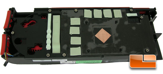
Taking the heat sink off is a simple task with the appropriate tools. The entire assembly comes apart with eighteen screws. Eleven on the back plate, four at the four sides of the RV870 chip and three by the Display ports.

You can see the copper contact point of the heat sink and the thermal tape used to make contact on all the other points that need to be cooled. Another six screws and you can pull the front shroud off and reveal the rest of the heat sink.

In order to keep the HD5870 cool it HIS Utilizes the reference cooler. The reference cooler uses four heat pipes that run through the aluminum fins and air is fed through the heat sink assembly via a blower at the back of the card.

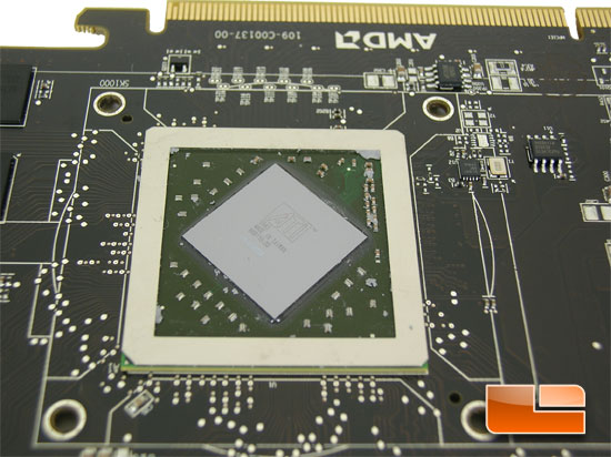
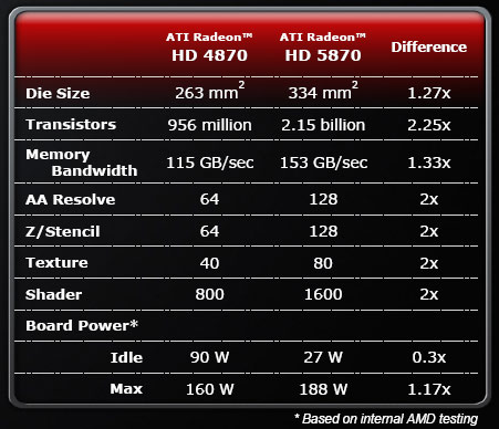
Above is the heart of the HIS Radeon HD5870. The RV870 also called the cypress core is the most advanced graphics core to date. Built on 40nm technology it possesses 2.15 billion transistors which is 2.25x the amount of transistors found on the HD4870.

As you can see in the above slide the technology in the HD5870 is a huge leap from the HD4870. Despite the huge differences in technology and presumably performance, the HD5870 utilizes only 28 more watts under full load than its predecessor(according to AMD).

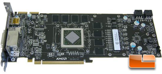
The front of the card is also home to the eight memory ic's. The memory chips are manufactured by Samsung and have a rated speed of 1250MHz though come set at 1200MHz. If you look toward's the right side of the card you can see a label with CPL2-4. I was curious what that was, so after a little digging I discovered that it is the 4 phase power inductor.
| Model Name | HIS HD 5870 (DirectX 11 / Eyefinity / Full HD 1080p) Native HDMI 1GB (256bit) GDDR5 Dual DL-DVI / Display Port / HDMI (HDCP) PCIe (RoHS) (DiRT-2)
|

Chipset | Radeon HD 5870 PCIe Series |

ASIC | Radeon HD 5870 GPU |

Pixel Pipelines | 1600 stream processing units* (Unified) |

Vertex Engines | 1600 stream processing units* (Unified) |

Manu. Process (Micron) | 40nm |

Transistor |
|

Memory Size (MB) | 1024 |

Memory Type | GDDR5 |

RAMDAC (MHz) | 400 |

Engine CLK (MHz) | 850
|

Memory CLK (Gbps) | 4.8Gbps
|

Memory Interface (bit) | 256 |

Max. Resolution | 3x 2560*1600 (Dual dual-link) |

Bus Interface | PCI Express x16 |

Display Port
| Yes |

HDMI | Yes |

DVI | Yes |

2nd DVI | Yes |
Read on to see what type of toys come with the HIS Radeon HD5870


